![]()
by Rick McLeod, Developer Technical Program
The next-generation systems from Silicon Graphics® will include PCI bus technology. Although you can write a device driver for just about any PCI card, the card may not operate efficiently with Silicon Graphics systems if it was designed specifically for the PC architecture. To take advantage of this technology, you need to understand both the PCI bus as well as the architecture of the system to which it connects. Read this article to learn about some key hardware concepts that will help you to prepare for the PCI bus as it is implemented in the next-generation systems.
The PCI Bus Specification details how the bus operates, but it does not mention anything about the architecture of the systems to which the bus connects. Many of the today's PCI cards are designed for the PC architecture. However, you also need to understand the architecture of the connected system, because it affects hardware design decisions such as on-board buffering and whether the board is a slave or bus master.
Comparing the PC architecture to the architecture of one of Silicon Graphics' next-generation systems brings this issue into focus. Figure 1 shows the architecture of a typical PC that includes the PCI bus. The PCI bus is drawn with heavy lines on the diagram to highlight the fact that the PCI bus is very close to the CPU and memory.
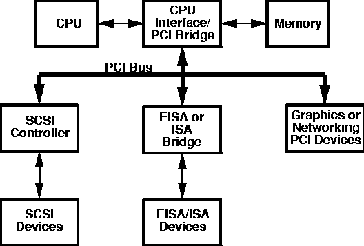
A private bus usually connects the CPU and memory; it also connects the ASIC that acts as a memory controller, CPU interface, and bridge to the PCI bus. This arrangement makes the PCI bus a secondary bus. The PCI bus has three or four slots for add-in cards, and it has one or more on-board PCI devices. The diagram shows an on-board bridge between the PCI bus and the ISA bus, typically referred to as a legacy bus. A PCI-based SCSI controller controls a set of SCSI devices. In this case, both the ISA bus and SCSI bus are tertiary buses.
As a secondary bus, the PCI bus must traverse only one bridge/controller to get to memory, which minimizes the latency for memory contention. The tertiary buses, SCSI and ISA, must first contend with other devices for the PCI bus before they can gain access to memory through the bridge/controller ASIC. This increases the latency time for these devices.
Many of the PCI cards designed for use in the PC take advantage of the low memory access latency times by doing small accesses (reads and writes) to the PCI card's I/O space, rather than using the memory space of the card. Moreover, many PCI cards are slaves rather than bus masters.
Figure 2 shows the architecture of a next-generation system that incorporates the PCI bus. Again, the PCI bus has been drawn with heavy lines to highlight its placement within the overall architecture.
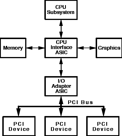
In this architecture the PCI bus is the tertiary bus. Contrast this with the PC architecture, which assigns the PCI bus as the secondary bus. As in the PC architecture, the memory access latency times for the tertiary bus are longer than for the secondary or primary buses.
Cards designed implicitly for the PC architecture may be slaves that use many small accesses to I/O space. Consequently, these cards will not work efficiently in the Silicon Graphics architecture. However, Silicon Graphics designed the bridges to the PCI bus to compensate for the longer latency times by incorporating features such as prefetch and bursts.
What factors are involved in making a PCI device perform well in a next-generation Silicon Graphics system? Silicon Graphics drafted a set of Good Citizenship Guidelines to answer this question. These guidelines are not intended to take the place of the PCI Bus Specification. Indeed, all boards for Silicon Graphics systems must be compliant with Version 2.1 of the specification. Rather, the guidelines augment the bus specification with the characteristics that work most efficiently with the Silicon Graphics architecture. The following sections provide an overview of these guidelines.
Plan for the time delay between when the board requests access to memory and when access to memory is granted. This affects the amount of on-board buffering for data. Designing for a latency of 100 microseconds accounts for the vast majority of system configurations.
Account for the time delay between when the board requests an interrupt and when this interrupt is serviced. This also affects the amount of on-board buffering for data. Interrupt service latency is typically around 1 millisecond.
Move data to and from the card by using DMA operations, since they are more efficient than I/O space operations. This implies that the card is a bus master that can do its own DMA operations. We discourage PIO operations as a method of moving large amounts of data. In other words, just say no to PIO!
Since interrupt latency is around 1 millisecond, minimize the number of interrupts the card generates.
The next-generation systems support both 32- and 64-bit-wide data paths. Use 64-bit data paths whenever possible, since twice the amount of data moves with each bus cycle.
The bridge ASICs are designed to work most efficiently with a burst size of 128 bytes aligned on 128-byte addresses. These ASICs disconnect transactions larger than 128 bytes at 128 bytes, which forces the board to initiate additional burst transactions.
Some processes do not use the bus as efficiently as they could. Two such examples include empty bytes in a burst (that is, the byte-enable bit for one or more bytes is not enabled) and transactions smaller than 128 bytes. Both of these situations cause extra bus and/or memory transactions, which slow the card's performance.
The bridge ASICs prefetch data for reads if you use the Multiple Read bus command. This command uses the prefetch capability in the bridge ASICs, counteracting the effects of a longer memory access latency time.
Some of the next-generation Silicon Graphics systems support 64-bit addresses. For these systems, it is best to use 64-bit addresses to avoid the delay in mapping 32-bit addresses to the larger address space. In addition, by using 64-bit addresses, you gain control over features like prefetching and byte swapping on a transaction-by-transaction basis.
The PCI bus provides the high bandwidth to the system many devices require: 132áMB/sec for the 32-bit-wide data path and 264 MB/sec for the 64-bit data path. By following the guidelines in this article and in the PCI Developer Guide, you can optimize the performance of both the system as well as the PCI device. The key to achieving these performance gains is to understand not only the PCI bus, but also the characteristics of the system to which the bus is connected.
The PCI Developer Guide goes into much more detail about the architecture of these new systems, the Good Citizenship Guidelines, and the features that take advantage of the PCI bus technology. You can obtain this document from the Developer Program. In addition, Club Dev will soon feature a section devoted to the PCI bus.


We welcome feedback and comments at
devprogram@sgi.com.